


A circuit board inside a wireless sensor and one inside an industrial power supply may look similar at first glance. Both carry components, connect circuits, and distribute power. Electrically, however, they can be dealing with very different problems.
As power levels rise, a PCB can no longer be treated simply as a platform for routing signals between components. The board itself becomes part of the power-delivery system. Trace resistance, copper thickness, temperature rise, connectors, vias, and even the way heat moves through the board can affect whether the product runs reliably.
That is why the PCBs used in high-power electronics often look quite different from those found in low-power consumer devices.
More Current Changes the Job of the PCB
Every copper trace has resistance. It may be very small, but it is never zero.
When current passes through that resistance, some electrical energy is converted into heat. Because resistive power loss increases with the square of current, a change that seems modest electrically can create a much larger thermal problem.
This is easy to overlook when moving from a low-current design to a higher-power version of the same product. A trace that works perfectly well at 1 A cannot automatically be expected to behave the same way at 10 A simply because the circuit topology has not changed.
Higher current can lead to:
- Greater voltage drop across power paths
- Higher trace temperatures
- Hot spots around vias, pads, and connectors
- Increased stress on solder joints and components
- Lower overall power efficiency
At this point, PCB layout is no longer just about fitting everything onto the board. The physical geometry of the copper becomes part of the electrical design.
Trace Width Is Usually the First Tool
One of the simplest ways to reduce the resistance of a PCB trace is to make it wider.
A wider trace has a larger copper cross-section, which allows it to carry current with less resistance. For many designs, this is all that is needed. Power traces are simply made wider than signal traces, while sensitive or low-current circuitry continues to use conventional routing.
The problem is space.
Modern electronics are rarely designed with unlimited PCB area. Power components, connectors, control circuitry, isolation distances, mounting holes, and thermal requirements are all competing for room.
At some point, making every high-current trace wider becomes impractical.
This is particularly noticeable in compact power supplies, motor controllers, battery systems, charging equipment, and other products where a significant amount of current has to move through a relatively small board.
That is where copper thickness becomes another design variable.
Also Read: brandrank.ai normalization transformation rules
When Copper Thickness Starts to Matter
PCB copper is commonly specified by weight. One ounce of copper corresponds to roughly 35 µm of nominal copper thickness, while boards designed for substantially higher current may use several ounces of copper instead. Heavy copper PCBs are commonly associated with copper thicknesses of 3 oz or more.
Increasing copper thickness increases the cross-sectional area of a trace without requiring the same increase in trace width.
When board space is limited and widening the power path is no longer practical, designers may use a heavy copper PCB construction to provide more copper for high-current sections of the circuit.
The idea is straightforward, but it is important not to think of thicker copper as a universal upgrade. It changes the way the PCB has to be designed and manufactured.
Thicker Copper Comes With Trade-Offs
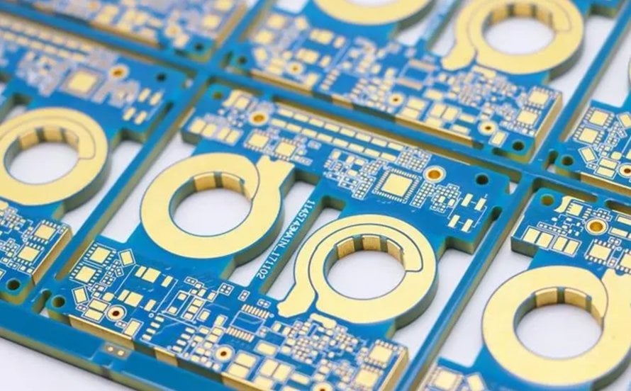
Adding more copper helps with current handling, but it makes fine PCB geometry more difficult to manufacture.
PCB traces are formed through imaging and etching processes. As the copper gets thicker, maintaining very narrow traces and gaps becomes more challenging. Manufacturer design rules therefore tend to become less aggressive as copper thickness increases. NCAB’s published heavy-copper capabilities, for example, show progressively larger trace and gap requirements as copper weight increases from 3 oz to 6 oz.
That creates an important design trade-off.
A board may need thick copper for its power section while simultaneously needing fine routing around controllers, gate drivers, sensors, or communication circuitry.
Designers therefore have to think carefully about where the extra copper is actually needed rather than simply specifying the heaviest copper available across the entire board.
In some products, different copper requirements may even influence the layer stackup or lead to more specialized PCB constructions.
Heat Does Not Disappear Just Because the Copper Is Thicker
Another common mistake is to treat heavy copper as a complete thermal-management solution.
Copper is highly thermally conductive, so increasing its cross-section can help spread heat and reduce resistive heating along a power path. Heavy copper is therefore commonly used as one part of thermal-management strategies in high-power PCB applications.
But heat still has to go somewhere.
If a MOSFET, power diode, regulator, or other component is generating significant heat, the PCB still needs a path to move that heat away from the device and eventually into the surrounding environment.
Depending on the product, that may involve thermal vias, larger copper areas, heatsinks, metal inserts, airflow, enclosure design, or other thermal-management methods.
The important point is that electrical design and thermal design become increasingly difficult to separate as power density rises.
A trace may be electrically capable of carrying the required current but still produce an unacceptable local temperature rise. Likewise, a component may operate within its electrical rating while running too hot because the surrounding PCB cannot move heat away effectively.
Vias Can Become the Hidden Bottleneck
Wide or thick copper traces do not help much if the current has to pass through an inadequate via structure.
This becomes especially important when power moves between PCB layers.
A via carries current through the copper plated onto the wall of the drilled hole. If a high-current path changes layers, the designer may need multiple vias, larger holes, heavier plating, or another interconnection strategy to prevent that transition from becoming the narrowest point in the current path.
The same principle applies throughout the board.
A high-current circuit should be thought of as a complete path rather than a collection of individual traces. The effective bottleneck may be a trace, via, pad, connector, solder joint, or terminal.
Strengthening only one part of that path does not automatically improve the rest.
Connectors Matter More Than They First Appear
Connectors are another area where high-power PCB designs can run into trouble.
A power connector may have a current rating that looks adequate on paper, but the PCB footprint and the copper surrounding it still have to carry that current away from the connector.
If a large terminal feeds into a narrow neck of copper, the design has simply moved the bottleneck from the connector contact to the PCB.
There is also a mechanical aspect to consider. Larger power cables and connectors can put more stress on solder joints and plated holes, particularly in products exposed to vibration, repeated plugging, or field servicing.
For this reason, power connector selection and PCB layout should be considered together rather than as separate design tasks.
Also Read: themes android pie
High Current and High Voltage Are Not the Same Problem
High-power electronics can involve high current, high voltage, or both, but those conditions place different demands on a PCB.
High-current design focuses heavily on conductor resistance, copper cross-section, temperature rise, vias, and connection points.
High-voltage design introduces another set of concerns, including spacing, creepage, clearance, insulation, contamination, and dielectric strength.
A board used in power electronics may need to satisfy both sets of requirements at the same time.
This is one reason power PCB design often becomes much more than simply increasing trace width. Changes made to improve current handling must still leave enough physical separation for voltage requirements and enough room for the rest of the circuit.
How Do You Know When a Standard PCB Is No Longer Enough?
There is no single current value at which every design suddenly needs heavier copper.
The answer depends on the entire system: allowable temperature rise, trace length, available board area, layer structure, airflow, ambient temperature, duty cycle, and the amount of current each part of the circuit actually carries.
A better question is whether a conventional copper weight still allows the required current paths to fit on the board while meeting the electrical and thermal targets.
If it does, there may be little reason to complicate the PCB.
If the power traces are becoming excessively wide, temperature rise is difficult to control, or the PCB is consuming too much area simply to distribute current, heavier copper becomes worth evaluating.
This decision should ideally be made before the layout is finished. Moving to substantially thicker copper later can affect trace spacing, stackup, vias, and manufacturing rules, which may force parts of the board to be redesigned.
The PCB Is Part of the Power System
As electronics become smaller and more power-dense, PCB design increasingly sits at the intersection of electrical, thermal, and mechanical engineering.
The copper that once looked like little more than a way to connect components can become a major part of the product’s power-distribution and thermal strategy.
That does not mean every high-power product needs an exotic PCB. Often, careful trace sizing, sensible component placement, good via design, and effective cooling are enough. Engineers working with higher current levels should consider all of these factors together, since good high-current PCB design is ultimately about managing the entire current and heat path rather than solving one problem in isolation.
But as current and power density rise, the margin for treating the board as an afterthought gets smaller.
In high-power electronics, the PCB is not simply holding the power circuit together. It is part of the power circuit.